Page top

Building Automation


Industrial Automation


Power Automation & Safety

Bangladesh Distributor

CJ1W-ID / IA

CJ-series Input Units

CJ1W-ID / IA

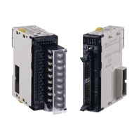
A wide range of CJ series input units are available featuring high-speed input and suitability for various applications. This unit is available for CJ/NJ controllers.

about this Product Family

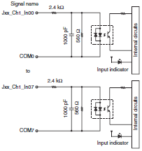
CJ1W-ID201 DC Input Unit (12 to 24-VDC, 8 Points)

Name 8-point DC Input Unit with Terminal Block
Model CJ1W-ID201
Rated Input Voltage 12 to 24 VDC
Rated Input Voltage Range 10.2 to 26.4 VDC
Input Impedance 2.4 kΩ
Input Current 10 mA typical (at 24 VDC)
ON Voltage/ON Current 8.8 VDC min./3 mA min.
OFF Voltage/OFF Current 3 VDC max./1 mA max.
ON Response Time 8.0 ms max. (Can be set to between 0 and 32 ms in the Setup.) *1
OFF Response Time 8.0 ms max. (Can be set to between 0 and 32 ms in the Setup.) *1
Number of Circuits 8 independent circuits
Number of Simultaneously
ON Points
100% simultaneously ON
Insulation Resistance 20 MΩ min. between external terminals and the GR terminal (100 VDC)
Dielectric Strength 1,000 VAC between the external terminals and the GR terminal for 1 minute at a leakage current of
10 mA max.
Internal Current Consumption 80 mA max.
Weight 110 g max.
Circuit Configuration
2054_sp_1_1
The signal names of the terminals are the device variable names.
The device variable names are the names that use "Jxx" as the device name.
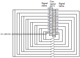
External connection and
terminal-device variable
diagram
2054_sp_1_2
Polarity of the input power supply can be connected in either direction.
The signal names of the terminals are the device variable names.
The device variable names are the names that use "Jxx" as the device name.

*1. The ON response time will be 20 μs maximum and OFF response time will be 400 μs maximum even if the response
       time are set to 0 ms due to internal element delays.
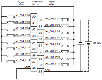
*2. Terminal numbers A0 to A8 and B0 to B8 are used in the external connection and terminal-device variable diagrams.
       They are not printed on the Units.
Note: Although 16 I/O bits (1 word) are allocated, only 8 of these can be used for external I/O.

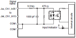
CJ1W-ID211 DC Input Unit (24 VDC, 16 Points)

Name 16-point DC Input Unit with Terminal Block
Model CJ1W-ID211
Rated Input Voltage 24 VDC
Rated Input Voltage Range 20.4 to 26.4 VDC
Input Impedance 3.3 kΩ
Input Current 7 mA typical (at 24 VDC)
ON Voltage/ON Current 14.4 VDC min./3 mA min.
OFF Voltage/OFF Current 5 VDC max./1 mA max.
ON Response Time 8.0 ms max. (Can be set to between 0 and 32 ms in the Setup.) *1
OFF Response Time 8.0 ms max. (Can be set to between 0 and 32 ms in the Setup.) *1
Number of Circuits 16 (16 points/common, 1 circuit)
Number of Simultaneously
ON Points
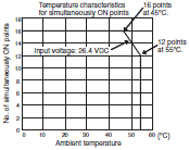
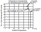
100% simultaneously ON (at 24 VDC) (Refer to the following illustration.)
Insulation Resistance 20 MΩ min. between external terminals and the GR terminal (100 VDC)
Dielectric Strength 1,000 VAC between the external terminals and the GR terminal for 1 minute at a leakage current of
10 mA max.
Internal Current Consumption 80 mA max.
Weight 110 g max.
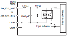
Circuit Configuration
2054_sp_2_1
The signal names of the terminals are the device
variable names.
The device variable names are the names that use
"Jxx" as the device name.
2054_sp_2_2
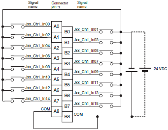
External connection and
terminal-device variable
diagram
2054_sp_2_3
Polarity of the input power supply can be connected in either direction.
The signal names of the terminals are the device variable names.
The device variable names are the names that use "Jxx" as the device name.

*1. The ON response time will be 20 μs maximum and OFF response time will be 400 μs maximum even if the response
       time are set to 0 ms due to internal element delays.
*2. Terminal numbers A0 to A8 and B0 to B8 are used in the external connection and terminal-device variable diagrams.
       They are not printed on the Units.

CJ1W-ID212 DC Input Unit (24 VDC, 16 Points)

Name 16-point DC Input Unit with Terminal Block
Model CJ1W-ID212
Rated Input Voltage 24 VDC
Rated Input Voltage Range 20.4 to 26.4 VDC
Input Impedance 3.3 kΩ
Input Current 7 mA typical (at 24 VDC)
ON Voltage/ON Current 14.4 VDC min./3 mA min.
OFF Voltage/OFF Current 5 VDC max./1 mA max.
ON Response Time 8.0 ms max. (Can be set to between 0 and 32 ms in the Setup.) *1
OFF Response Time 8.0 ms max. (Can be set to between 0 and 32 ms in the Setup.) *1
Number of Circuits 16 (16 points/common, 1 circuit)
Number of Simultaneously
ON Points
100% simultaneously ON (at 24 VDC) (Refer to the following illustration.)
Insulation Resistance 20 MΩ min. between external terminals and the GR terminal (100 VDC)
Dielectric Strength 1,000 VAC between the external terminals and the GR terminal for 1 minute at a leakage current of
10 mA max.
Internal Current Consumption 130 mA max.
Weight 110 g max.
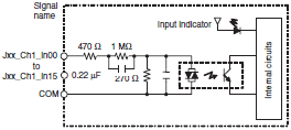
Circuit Configuration
2054_sp_3_1
The signal names of the terminals are the device
variable names.
The device variable names are the names that use
"Jxx" as the device name.
2054_sp_3_2
External connection and
terminal-device variable
diagram
2054_sp_3_3
Polarity of the input power supply can be connected in either direction.
The signal names of the terminals are the device variable names.
The device variable names are the names that use "Jxx" as the device name.

*1. The ON response time will be 15 μs maximum and OFF response time will be 90 μs maximum even if the response
       time are set to 0 ms due to internal element delays.
*2. Terminal numbers A0 to A8 and B0 to B8 are used in the external connection and terminal-device variable diagrams.
       They are not printed on the Units.

CJ1W-ID231 DC Input Unit (24 VDC, 32 Points)

Name 32-point DC Input Unit with Fujitsu Connector
Model CJ1W-ID231
Rated Input Voltage 24 VDC
Rated Input Voltage Range 20.4 to 26.4 VDC
Input Impedance 5.6 kΩ
Input Current 4.1 mA typical (at 24 VDC)
ON Voltage/ON Current 19.0 VDC min./3 mA min.
OFF Voltage/OFF Current 5 VDC max./1 mA max.
ON Response Time 8.0 ms max. (Can be set to between 0 and 32 in the Setup.) *
OFF Response Time 8.0 ms max. (Can be set to between 0 and 32 in the Setup.) *
Number of Circuits 32 (16 points/common, 2 circuits)
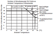
Number of Simultaneously
ON Points
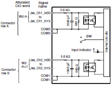
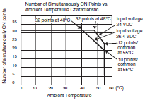
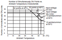
75% (12 points/common) simultaneously ON (at 24 VDC) (Refer to the following illustration.)
Insulation Resistance 20 MΩ min. between external terminals and the GR terminal (100 VDC)
Dielectric Strength 1,000 VAC between the external terminals and the GR terminal for 1 minute at a leakage current of
10 mA max.
Internal Current Consumption 90 mA max.
Weight 70 g max.
Accessories None
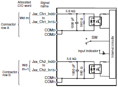
Circuit Configuration
2054_sp_4_1
The signal names of the terminals are the device
variable names.
The device variable names are the names that use
"Jxx" as the device name.
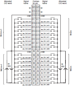
2054_sp_4_2
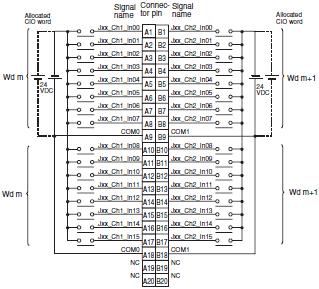
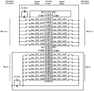
External connection and
terminal-device variable
diagram
2054_sp_4_3
The input power polarity can be connected in either direction.
Be sure to wire both pins A9 and A18 (COM0), and set the same polarity for both pins.
Be sure to wire both pins B9 and B18 (COM1), and set the same polarity for both pins.
The signal names of the terminals are the device variable names.
The device variable names are the names that use "Jxx" as the device name.

* The ON response time will be 20 μs maximum and OFF response time will be 400 μs maximum even if the response
    times are set to 0 ms due to internal element delays.
Note: Observe the following restrictions when connecting to a 2-wire sensor.
           • Make sure the input power supply voltage is larger than the ON voltage (19 V) plus the residual voltage of the
               sensor (approx. 3 V).
           • Use a sensor with a minimum load current of 3 mA min.
           • Connect bleeder resistance if you connect a sensor with a minimum load current of 5 mA or higher.

CJ1W-ID232 DC Input Unit (24 VDC, 32 Points)

Name 32-point DC Input Unit with MIL Connector
Model CJ1W-ID232
Rated Input Voltage 24 VDC
Rated Input Voltage Range 20.4 to 26.4 VDC
Input Impedance 5.6 kΩ
Input Current 4.1 mA typical (at 24 VDC)
ON Voltage/ON Current 19.0 VDC min./3 mA min.
OFF Voltage/OFF Current 5 VDC max./1 mA max.
ON Response Time 8.0 ms max. (Can be set to between 0 and 32 in the Setup.) *
OFF Response Time 8.0 ms max. (Can be set to between 0 and 32 in the Setup.) *
Number of Circuits 32 (16 points/common, 2 circuits)
Number of Simultaneously
ON Points
75% (12 points/common) simultaneously ON (at 24 VDC) (Refer to the following illustration.)
Insulation Resistance 20 MΩ min. between external terminals and the GR terminal (100 VDC)
Dielectric Strength 1,000 VAC between the external terminals and the GR terminal for 1 minute at a leakage current of
10 mA max.
Internal Current Consumption 90 mA max.
Weight 70 g max.
Accessories None
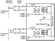
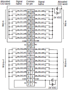
Circuit Configuration
2054_sp_5_1
The signal names of the terminals are the device
variable names.
The device variable names are the names that use
"Jxx" as the device name.
2054_sp_5_2
External connection and
terminal-device variable
diagram
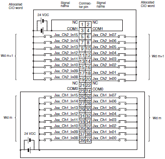
2054_sp_5_3
The input power polarity can be connected in either direction.
Be sure to wire both pins 23 and 24 (COM0), and set the same polarity for both pins.
Be sure to wire both pins 3 and 4 (COM1), and set the same polarity for both pins.
The signal names of the terminals are the device variable names.
The device variable names are the names that use "Jxx" as the device name.

* The ON response time will be 20 μs maximum and OFF response time will be 400 μs maximum even if the response
    times are set to 0 ms due to internal element delays.
Note: Observe the following restrictions when connecting to a 2-wire sensor.
          • Make sure the input power supply voltage is larger than the ON voltage (19 V) plus the residual voltage of the
              sensor (approx. 3 V).
          • Use a sensor with a minimum load current of 3 mA min.
          • Connect bleeder resistance if you connect a sensor with a minimum load current of 5 mA or higher.

CJ1W-ID233 DC Input Unit (24 VDC, 32 Points)

Name 32-point DC Input Unit with MIL Connector
Model CJ1W-ID233
Rated Input Voltage 24 VDC
Rated Input Voltage Range 20.4 to 26.4 VDC
Input Impedance 5.6 kΩ
Input Current 4.1 mA typical (at 24 VDC)
ON Voltage/ON Current 19.0 VDC min./3 mA min.
OFF Voltage/OFF Current 5 VDC max./1 mA max.
ON Response Time 8.0 ms max. (Can be set to between 0 and 32 in the Setup.) *
OFF Response Time 8.0 ms max. (Can be set to between 0 and 32 in the Setup.) *
Number of Circuits 32 (16 points/common, 2 circuits)
Number of Simultaneously
ON Points
75% (12 points/common) simultaneously ON (at 24 VDC) (Refer to the following illustration.)
Insulation Resistance 20 MΩ min. between external terminals and the GR terminal (100 VDC)
Dielectric Strength 1,000 VAC between the external terminals and the GR terminal for 1 minute at a leakage current of
10 mA max.
Internal Current Consumption 200 mA max.
Weight 70 g max.
Accessories None
Circuit Configuration
2054_sp_6_1
The signal names of the terminals are the device
variable names.
The device variable names are the names that use
"Jxx" as the device name.
2054_sp_6_2
External connection and
terminal-device variable
diagram
2054_sp_6_3
The input power polarity can be connected in either direction.
Be sure to wire both pins 23 and 24 (COM0), and set the same polarity for both pins.
Be sure to wire both pins 3 and 4 (COM1), and set the same polarity for both pins.
The signal names of the terminals are the device variable names.
The device variable names are the names that use "Jxx" as the device name.

* The ON response time will be 15 μs maximum and OFF response time will be 90 μs maximum even if the response
    times are set to 0 ms due to internal element delays.
Note: Observe the following restrictions when connecting to a 2-wire sensor.
          • Make sure the input power supply voltage is larger than the ON voltage (19 V) plus the residual voltage of the
              sensor (approx. 3 V).
          • Use a sensor with a minimum load current of 3 mA min.
          • Connect bleeder resistance if you connect a sensor with a minimum load current of 5 mA or higher.

CJ1W-ID261 DC Input Unit (24 VDC, 64 Points)

Name 64-point DC Input Unit with Fujitsu Connector
Model CJ1W-ID261
Rated Input Voltage 24 VDC
Rated Input Voltage Range 20.4 to 26.4 VDC
Input Impedance 5.6 kΩ
Input Current 4.1 mA typical (at 24 VDC)
ON Voltage/ON Current 19.0 VDC min./3 mA min.
OFF Voltage/OFF Current 5 VDC max./1 mA max.
ON Response Time 8.0 ms max. (Can be set to between 0 and 32 in the Setup.) *
OFF Response Time 8.0 ms max. (Can be set to between 0 and 32 in the Setup.) *
Number of Circuits 64 (16 points/common, 4 circuits)
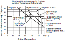
Number of Simultaneously
ON Points
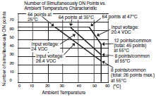
50% (16 points/common) simultaneously ON (at 24 VDC) (Refer to the following illustrations.)
Insulation Resistance 20 MΩ min. between external terminals and the GR terminal (100 VDC)
Dielectric Strength 1,000 VAC between the external terminals and the GR terminal for 1 minute at a leakage current of
10 mA max.
Internal Current Consumption 90 mA max.
Weight 110 g max.
Accessories None
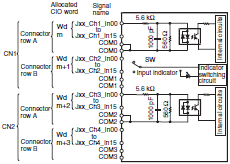
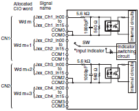
Circuit Configuration
2054_sp_7_1
The signal names of the terminals are the device
variable names.
The device variable names are the names that use
"Jxx" as the device name.
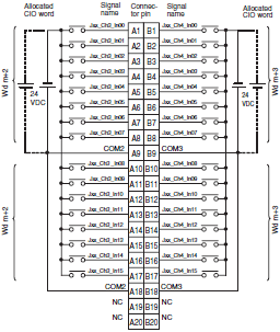
2054_sp_7_2
External connection and
terminal-device variable
diagram
CN1 CN2
2054_sp_7_3
The input power polarity can be connected in either
direction.
Be sure to wire both pins A9 and A18 (COM0) of
CN1, and set the same polarity for both pins.
Be sure to wire both pins B9 and B18 (COM1) of
CN1, and set the same polarity for both pins.
The signal names of the terminals are the device
variable names.
The device variable names are the names that use
"Jxx" as the device name.
2054_sp_7_4
The input power polarity can be connected in either
direction.
Be sure to wire both pins A9 and A18 (COM2) of
CN2, and set the same polarity for both pins.
Be sure to wire both pins B9 and B18 (COM3) of
CN2, and set the same polarity for both pins.
The signal names of the terminals are the device
variable names.
The device variable names are the names that use
"Jxx" as the device name.

* The ON response time will be 120 μs maximum and OFF response time will be 400 μs maximum even if the response
    times are set to 0 ms due to internal element delays.
Note: Observe the following restrictions when connecting to a 2-wire sensor.
          • Make sure the input power supply voltage is larger than the ON voltage (19 V) plus the residual voltage of the
              sensor (approx. 3 V).
          • Use a sensor with a minimum load current of 3 mA min.
          • Connect bleeder resistance if you connect a sensor with a minimum load current of 5 mA or higher.

CJ1W-ID262 DC Input Unit (24 VDC, 64 Points)

Name 64-point DC Input Unit with MIL Connector
Model CJ1W-ID262
Rated Input Voltage 24 VDC
Rated Input Voltage Range 20.4 to 26.4 VDC
Input Impedance 5.6 kΩ
Input Current 4.1 mA typical (at 24 VDC)
ON Voltage/ON Current 19.0 VDC min./3 mA min.
OFF Voltage/OFF Current 5 VDC max./1 mA max.
ON Response Time 8.0 ms max. (Can be set to between 0 and 32 in the Setup.) *
OFF Response Time 8.0 ms max. (Can be set to between 0 and 32 in the Setup.) *
Number of Circuits 64 (16 points/common, 4 circuits)
Number of Simultaneously
ON Points
50% (8 points/common) simultaneously ON (at 24 VDC) (Refer to the following illustrations.)
Insulation Resistance 20 MΩ min. between external terminals and the GR terminal (100 VDC)
Dielectric Strength 1,000 VAC between the external terminals and the GR terminal for 1 minute at a leakage current of
10 mA max.
Internal Current Consumption 90 mA max.
Weight 110 g max.
Accessories None
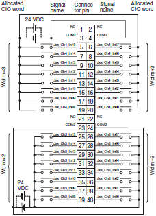
Circuit Configuration
2054_sp_8_1
The signal names of the terminals are the device
variable names.
The device variable names are the names that use
"Jxx" as the device name.
2054_sp_8_2
External connection and
terminal-device variable
diagram
CN1 CN2
2054_sp_8_3
The input power polarity can be connected in
either direction.
Be sure to wire both pins 23 and 24 (COM0) of
CN1, and set the same polarity for both pins.
Be sure to wire both pins 3 and 4 (COM1) of CN1,
and set the same polarity for both pins.
The signal names of the terminals are the device
variable names.
The device variable names are the names that use
"Jxx" as the device name.
2054_sp_8_4
The input power polarity can be connected in
either direction.
Be sure to wire both pins 23 and 24 (COM2) of
CN2, and set the same polarity for both pins.
Be sure to wire both pins 3 and 4 (COM3) of CN2,
and set the same polarity for both pins.
The signal names of the terminals are the device
variable names.
The device variable names are the names that use
"Jxx" as the device name.

* The ON response time will be 120 μs maximum and OFF response time will be 400 μs maximum even if the response
    times are set to 0 ms due to internal element delays.
Note: Observe the following restrictions when connecting to a 2-wire sensor.
          • Make sure the input power supply voltage is larger than the ON voltage (19 V) plus the residual voltage of the
              sensor (approx. 3 V).
          • Use a sensor with a minimum load current of 3 mA min.
          • Connect bleeder resistance if you connect a sensor with a minimum load current of 5 mA or higher.

CJ1W-IA201 AC Input Unit (200 VAC, 8 Points)

Name 8-point AC Input Unit with Terminal Block
Model CJ1W-IA201
Rated Input Voltage 200 to 240 VAC 50/60 Hz
Rated Input Voltage Range 170 to 264 VAC
Input Impedance 21 kΩ (50 Hz), 18 kΩ (60 Hz)
Input Current 9 mA typical (at 200 VAC, 50 Hz), 11 mA typical (at 200 VAC, 60 Hz)
ON Voltage/ON Current 120 VAC min./4 mA min.
OFF Voltage/OFF Current 40 VAC max./2 mA max.
ON Response Time 18.0 ms max. (default setting: 8 ms) *1
OFF Response Time 48.0 ms max. (default setting: 8 ms) *1
Number of Circuits 8 (8 points/common, 1 circuit)
Number of Simultaneously
ON Points
100% (8 points/common) simultaneously ON
Insulation Resistance 20 MΩ min. between external terminals and the GR terminal (500 VDC)
Dielectric Strength 2,000 VAC between the external terminals and the GR terminal for 1 minute at a leakage current of
10 mA max.
Internal Current Consumption 80 mA max.
Weight 130 g max.
Accessories None
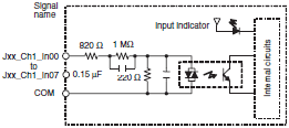
Circuit Configuration
2054_sp_9_1
The signal names of the terminals are the device variable names.
The device variable names are the names that use "Jxx" as the device name.
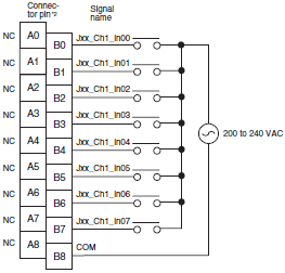
External connection and
terminal-device variable
diagram
2054_sp_9_2
The signal names of the terminals are the device variable names.
The device variable names are the names that use "Jxx" as the device name.

*1. Can be set to 0 ms, 0.5 ms, 1 ms, 2 ms, 4 ms, 8 ms, 16 ms, or 32 ms in the settings. When the response times have
       been set to 0 ms, the ON response time will be 10 ms maximum and the OFF response time will be 55 ms maximum
       due to internal element delays.
*2. Terminal numbers A0 to A8 and B0 to B8 are used in the external connection and terminal-device variable diagrams.
       They are not printed on the Units.
Note: Although 16 I/O bits (1 word) are allocated, only 8 of these can be used for external I/O.

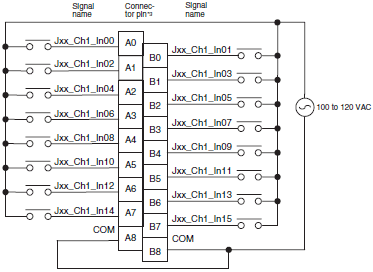
CJ1W-IA111 AC Input Unit (100 VAC, 16 points)

Name 16-point AC Input Unit with Terminal Block
Model CJ1W-IA111
Rated input voltage 100 to 120 VAC 50/60 Hz *2
Rated Input Voltage Range 85 to 132 VAC
Input Impedance 14.5 kΩ (50 Hz), 12 kΩ (60 Hz)
Input Current 7 mA typical (at 100 VAC, 50 Hz), 8 mA typical (at 100 VAC, 60 Hz)
ON Voltage/ON Current 70 VAC min./4 mA min
OFF Voltage/OFF Current 20 VAC max./2 mA max
ON Response Time 18 ms max. (default setting: 8 ms) *1
OFF Response Time 48 ms max. (default setting: 8 ms) *1
Number of Circuits 16 (16 points/common, 1 circuit)
Number of Inputs ON
Simultaneously
100% simultaneously ON (16 points/common)
Insulation Resistance 20 MΩ min. between external terminals and the GR terminal (500 VDC)
Dielectric Strength 2,000 VAC between the external terminals and the GR terminal for 1 minute at a leakage current of
10 mA max.
Internal Current Consumption 90 mA max.
Weight 130 g max.
Accessories None
Circuit Layout
2054_sp_10_1
The signal names of the terminals are the device variable names.
The device variable names are the names that use "Jxx" as the device name.
External connection and
terminal-device variable
diagram
2054_sp_10_2
The signal names of the terminals are the device variable names.
The device variable names are the names that use "Jxx" as the device name.

*1. Can be set to 0 ms, 0.5 ms, 1 ms, 2 ms, 4 ms, 8 ms, 16 ms, or 32 ms in the settings. When the response times have
       been set to 0 ms, the ON response time will be 10 ms maximum and the OFF response time will be 55 ms maximum
       due to internal element delays.
*2. Use an input voltage of 90 VAC or higher when connecting 2-wire sensors.
*3. Terminal numbers A0 to A8 and B0 to B8 are used in the external connection and terminal-device variable diagrams.
       They are not printed on the Units.

Bit Allocations for Input Unit

8-point Input Unit

Allocated CIO word Signal name (CJ/NJ)
CIO Bit
Wd m
(Input)
00 IN0/Jxx_Ch1_In00
01 IN1/Jxx_Ch1_In01
: :
06 IN6/Jxx_Ch1_In06
07 IN7/Jxx_Ch1_In07
08 -
09 -
: :
14 -
15 -

16-point Input Unit

Allocated CIO word Signal name (CJ/NJ)
CIO Bit
Wd m
(Input)
00 IN0/Jxx_Ch1_In00
01 IN1/Jxx_Ch1_In01
: :
14 IN14/Jxx_Ch1_In14
15 IN15/Jxx_Ch1_In15

32-point Input Unit

Allocated CIO word Signal name (CJ/NJ)
CIO Bit
Wd m
(Input)
00 IN0/Jxx_Ch1_In00
01 IN1/Jxx_Ch1_In01
: :
14 IN14/Jxx_Ch1_In14
15 IN15/Jxx_Ch1_In15
Wd m+1
(Input)
00 IN0/Jxx_Ch2_In00
01 IN1/Jxx_Ch2_In01
: :
14 IN14/Jxx_Ch2_In14
15 IN15/Jxx_Ch2_In15

64-point Input Unit

Allocated CIO word Signal name (CJ/NJ)
CIO Bit
Wd m
(Input)
00 IN0/Jxx_Ch1_In00
01 IN1/Jxx_Ch1_In01
: :
14 IN14/Jxx_Ch1_In14
15 IN15/Jxx_Ch1_In15
Wd m+1
(Input)
00 IN0/Jxx_Ch2_In00
01 IN1/Jxx_Ch2_In01
: :
14 IN14/Jxx_Ch2_In14
15 IN15/Jxx_Ch2_In15
Wd m+2
(Input)
00 IN0/Jxx_Ch3_In00
01 IN1/Jxx_Ch3_In01
: :
14 IN14/Jxx_Ch3_In14
15 IN15/Jxx_Ch3_In15
Wd m+3
(Input)
00 IN0/Jxx_Ch4_In00
01 IN1/Jxx_Ch4_In01
: :
14 IN14/Jxx_Ch4_In14
15 IN15/Jxx_Ch4_In15